- ●By fully utilizing the cleaning and drying technologies we have nurtured through our work with semiconductors and flat panels, we are able to accommodate a variety of needs, such as high quality, low damage, etc.
- ●We can realize space and utility saving through flexible design in accordance with objects to be cleaned, and needs.
- ●We can realize the removal of microscopic foreign matter through the combination of double-sided brushes, two-flow jets, pure-jets that apply ultrasonics, and high-pressure jets, etc.
- ●We can propose equipment that can handle wafer type and rectangular substrates in a wide variety of sizes.
- ●We can also produce dry processors (UV processing, etc.)
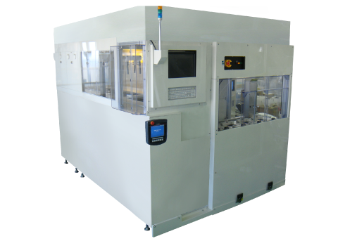
 Wafer spin processor
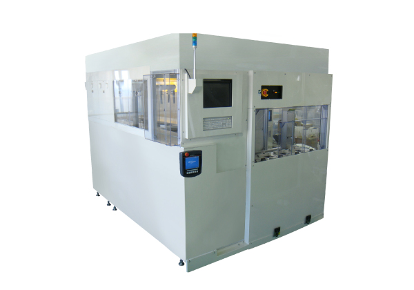
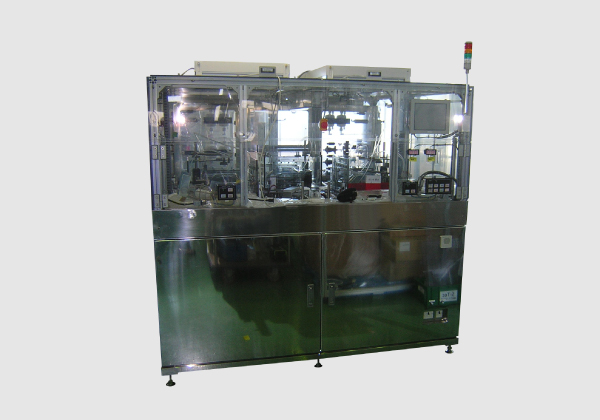
 UV processor
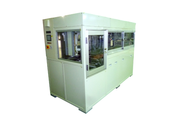
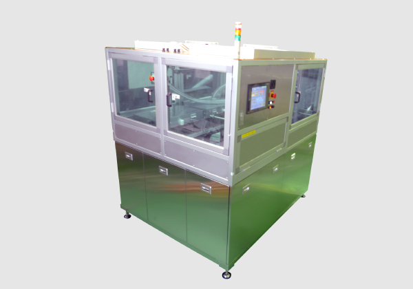
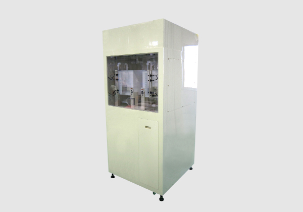
 Semi-automatic spin processor
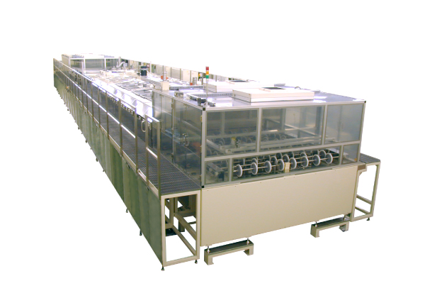
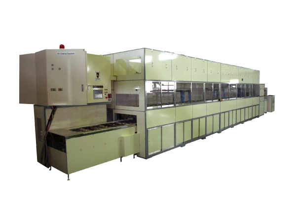
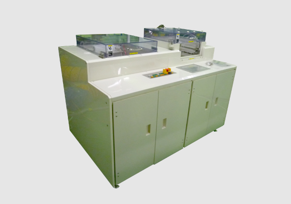
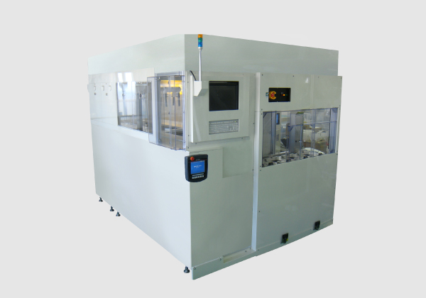 WET processor
 Automatic liquid chemical supply unit